- 您现在的位置:买卖IC网 > Sheet目录1993 > DS1110LE-125+ (Maxim Integrated Products)IC DELAY LINE 10TAP 14-TSSOP
DS1110L
3V 10-Tap Silicon Delay Line
2
______________________________________________________________________
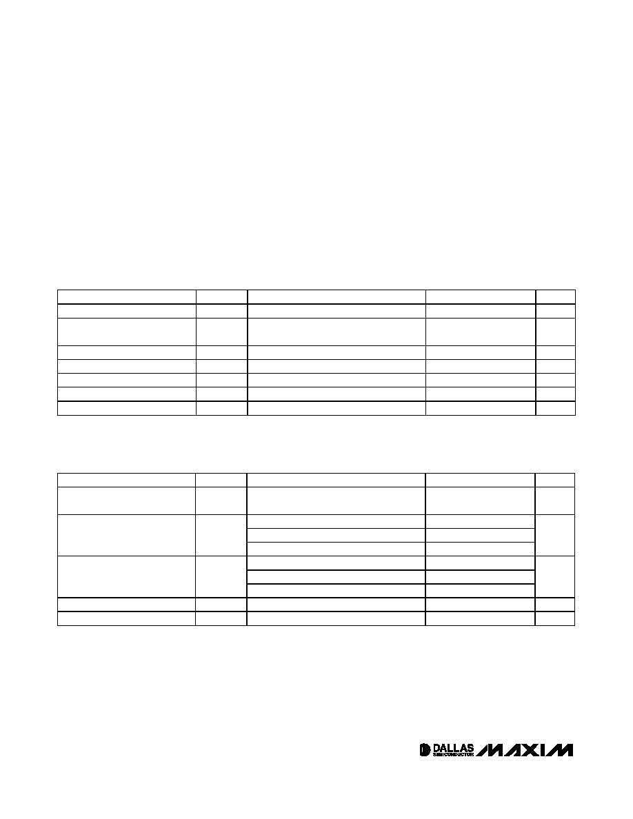
ABSOLUTE MAXIMUM RATINGS
DC ELECTRICAL CHARACTERISTICS
(-40°C to +85°C, VCC = 2.7V to 3.6V.)
Stresses beyond those listed under “Absolute Maximum Ratings” may cause permanent damage to the device. These are stress ratings only, and functional
operation of the device at these or any other conditions beyond those indicated in the operational sections of the specifications is not implied. Exposure to
absolute maximum rating conditions for extended periods may affect device reliability.
Voltage on Any Pin Relative to Ground .................-0.5V to +6.0V
Operating Temperature Range ...........................-40
°C to +85°C
Storage Temperature Range .............................-55
°C to +125°C
Soldering Temperature...................See IPC/JEDEC J-STD-020A
PARAMETER
SYMBOL
CONDITIONS
MIN
TYP
MAX
UNITS
Supply Voltage
VCC
(Note 1)
2.7
3.3
3.6
V
High-Level Input Voltage
VIH
(Note 1)
2.2
VCC
+ 0.3
V
Low-Level Input Voltage
VIL
(Note 1)
-0.3
+0.8
V
Input Leakage Current
II
0V
≤ VI ≤ VCC
-1.0
+1.0
A
Active Current
ICC
VCC = max, period = min (Note 2)
40
150
mA
High-Level Output Current
IOH
VCC = min, VOH = 2.3V
-1.0
mA
Low-Level Output Current
IOL
VCC = min, VOL = 0.5V
12
mA
AC ELECTRICAL CHARACTERISTICS
(-40°C to +85°C, VCC = 2.7V to 3.6V.)
PARAMETER
SYMBOL
CONDITIONS
MIN
TYP
MAX
UNITS
Input Pulse Width
tWI
(Note 6)
10% of
tap 10
ns
+25°C, 3.3V (Notes 3, 5, 6, 7, 9)
-2
Table 1
+2
0°C to +70°C (Notes 4–7)
-3
Table 1
+3
Input to Tap Delay
(Delays
≤ 40ns)
tPLH
tPHL
-40°C to +85°C (Notes 4–7)
-4
Table 1
+4
ns
+25°C, 3.3V (Notes 3, 5, 6, 7, 9)
-5
Table 1
+5
0°C to +70°C (Notes 4–7)
-8
Table 1
+8
Input to Tap Delay
(Delays > 40ns)
tPLH
tPHL
-40°C to +85°C (Notes 4–7)
-13
Table 1
+13
%
Power-Up Time
tPU
100
ms
Input Period
Period
(Note 8)
2 (tWI)ns
发布紧急采购,3分钟左右您将得到回复。
相关PDF资料
DS1110S-80+
IC DELAY LINE 10TAP 16-SOIC
DS1123LE-100+
IC DELAY LINE 256TAP 16-TSSOP
DS1124U-25+T
IC DELAY LINE 256TAP 10-USOP
DS1135LU-300/T&R
IC DELAY LINE 300NS 8-USOP
DS1135Z-12/T&R
IC DELAY LINE 12NS 8-SOIC
DS1181LE+
IC CLOCK MOD SS 8-TSSOP
DS1243Y-120
IC NVSRAM 64KBIT 120NS 28DIP
DS1244W-120IND
IC NVSRAM 256KBIT 120NS 28DIP
相关代理商/技术参数
DS1110LE-150
功能描述:延迟线/计时元素 RoHS:否 制造商:Micrel 功能:Active Programmable Delay Line 传播延迟时间:1000 ps 工作温度范围: 封装 / 箱体:QFN-24 封装:Tube
DS1110LE-150+
功能描述:延迟线/计时元素 3V 10-Tap Silicon Delay Line RoHS:否 制造商:Micrel 功能:Active Programmable Delay Line 传播延迟时间:1000 ps 工作温度范围: 封装 / 箱体:QFN-24 封装:Tube
DS1110LE-175
功能描述:延迟线/计时元素 RoHS:否 制造商:Micrel 功能:Active Programmable Delay Line 传播延迟时间:1000 ps 工作温度范围: 封装 / 箱体:QFN-24 封装:Tube
DS1110LE-175+
功能描述:延迟线/计时元素 3V 10-Tap Silicon Delay Line RoHS:否 制造商:Micrel 功能:Active Programmable Delay Line 传播延迟时间:1000 ps 工作温度范围: 封装 / 箱体:QFN-24 封装:Tube
DS1110LE-200
功能描述:延迟线/计时元素 3V 10-Tap Silicon Delay Line RoHS:否 制造商:Micrel 功能:Active Programmable Delay Line 传播延迟时间:1000 ps 工作温度范围: 封装 / 箱体:QFN-24 封装:Tube
DS1110LE-200+
功能描述:延迟线/计时元素 3V 10-Tap Silicon Delay Line RoHS:否 制造商:Micrel 功能:Active Programmable Delay Line 传播延迟时间:1000 ps 工作温度范围: 封装 / 箱体:QFN-24 封装:Tube
DS1110LE-200-W
功能描述:延迟线/计时元素 3V 10-Tap Silicon Delay Line RoHS:否 制造商:Micrel 功能:Active Programmable Delay Line 传播延迟时间:1000 ps 工作温度范围: 封装 / 箱体:QFN-24 封装:Tube
DS1110LE-250
功能描述:延迟线/计时元素 3V 10-Tap Silicon Delay Line RoHS:否 制造商:Micrel 功能:Active Programmable Delay Line 传播延迟时间:1000 ps 工作温度范围: 封装 / 箱体:QFN-24 封装:Tube